LoRa Mast Mount
A printed mount to replace the zip-ties-and-a-stick rig holding a LoRa node up: hold the board steady, keep the antenna vertical, protect the fragile coax connector, and take either a ground spike or a pole clamp on the same dovetail.
The node it replaces was zip-tied to a bamboo stick. That works, in the sense that a stick holds a radio up. It does not hold it in the same place twice, which is the part that matters when you are trying to measure coverage rather than measure how you happened to tie it on that day.
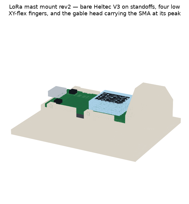
What it has to do
- Take the board as it is. The node is a bare board — see the correction below — so the mount has to hold a thin PCB by its edges without anything being unscrewed or removed.
- Leave the human parts reachable. The OLED stays visible and the USB-C, RST and PRG on the top edge stay accessible.
- Hold the whip vertical, and away from the board. The SMA bulkhead sits in an offset boss at the top so a knock to the antenna loads the printed post, not the connector on the board.
- Protect the u.FL. That connector's characteristic failure is a sharp bend right at the joint, so the pigtail runs in a captive channel with a generous radius and no tight turn at the connector end.
- Mount to whatever is there. One dovetail interface, two feet: a ground spike, and a clamp that still fits the original stick.
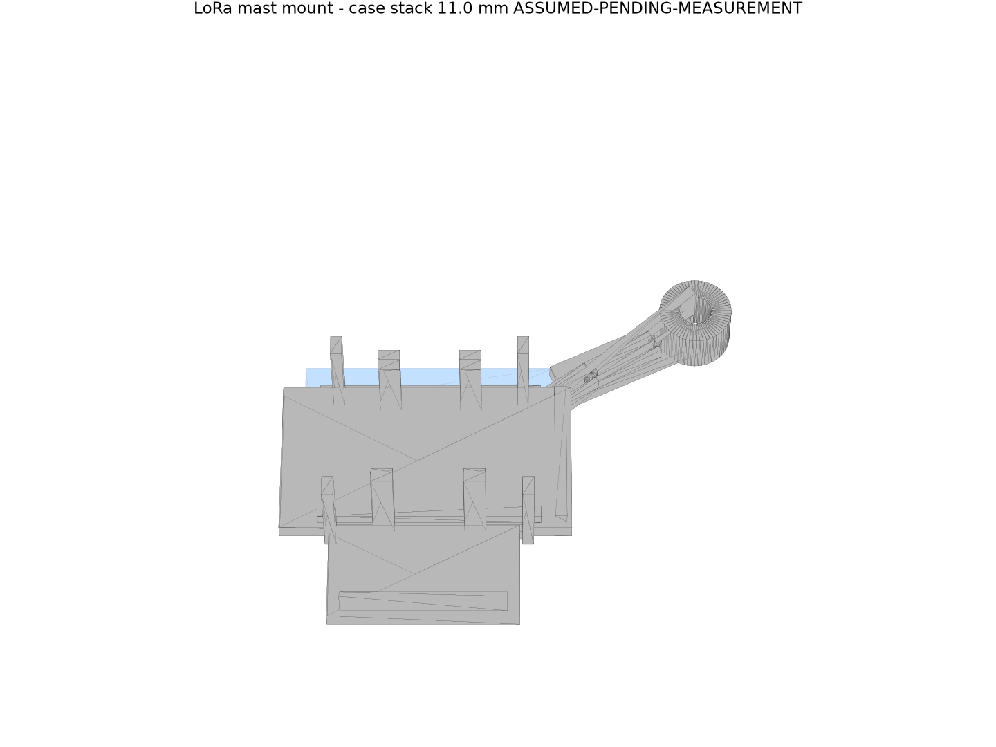
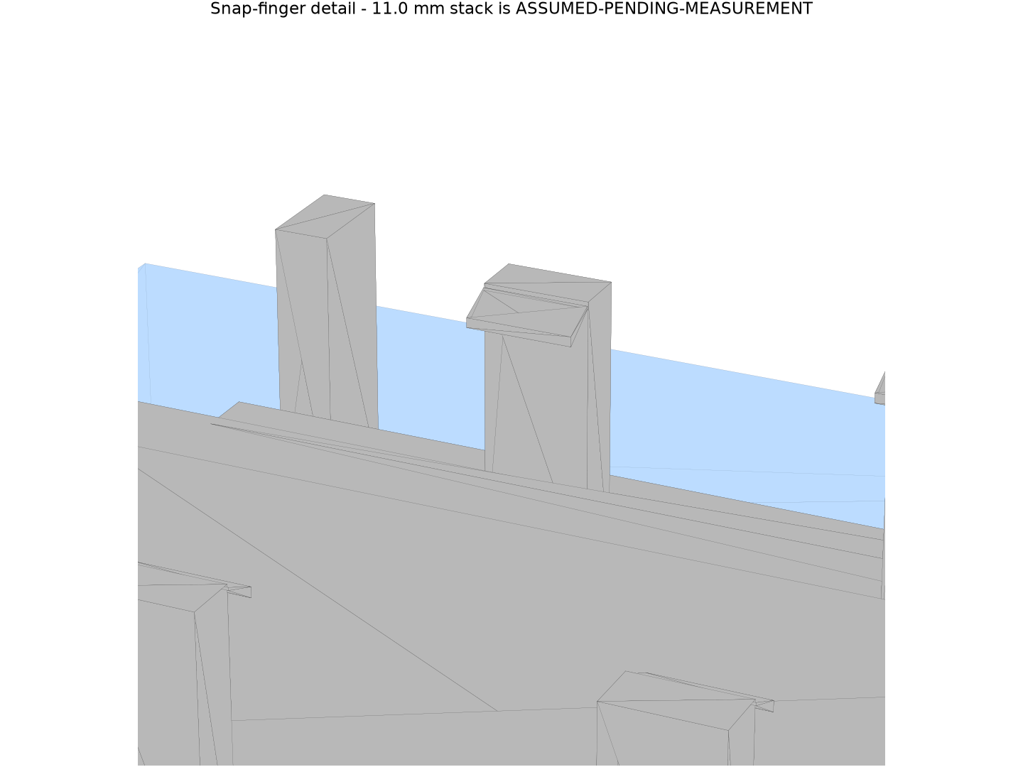
The snaps are calculated, not eyeballed
A snap fit that is over-strained does not fail honestly. It survives assembly, feels fine, and breaks on the third insertion — long after you have stopped suspecting it. So the fingers were sized from the cantilever strain relation rather than by feel. The arithmetic below stands; what it was applied to did not:
ε = 1.5 · t · y / L²
With a finger 1.60 mm thick and 12.00 mm long deflecting 0.85 mm to clear the case edge, strain works out to 1.42%. PETG's target for a part meant to flex repeatedly is 2%, so all four fingers sit comfortably under the limit with room for the real case to be slightly thicker than modelled.
Orientation matters as much as the arithmetic. The part prints with its back flat on the bed so the fingers flex across the extruded roads rather than peeling one layer off the next — a PETG snap printed the other way up delaminates no matter how good the strain number looks.
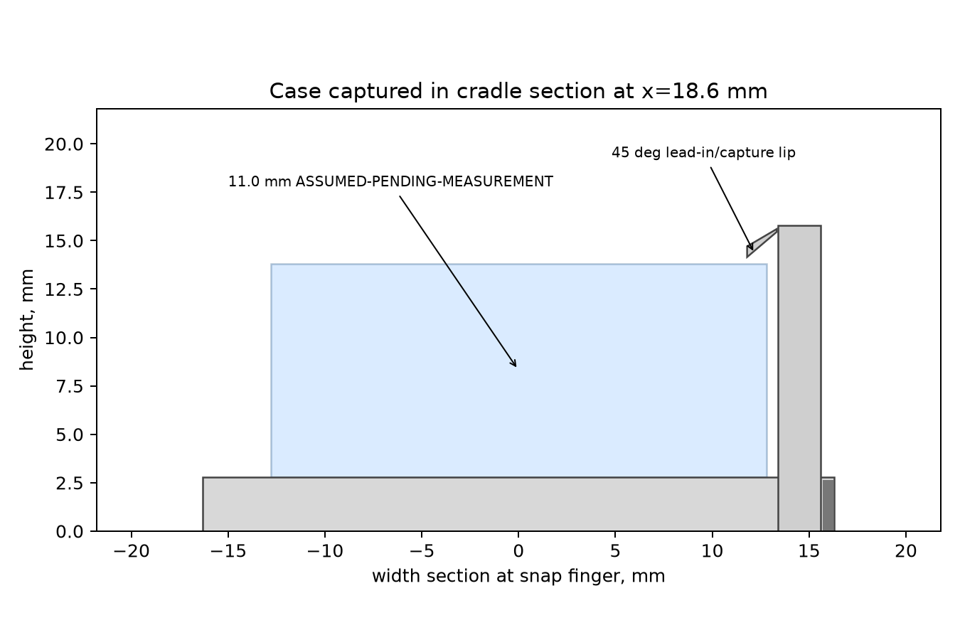
The correction: there is no case
This design was drawn from a brief describing the node as sitting in a clear acrylic sandwich — two plates and the board on standoffs, about 11 mm thick. The snap fingers were sized to grip that stack.
It is not what the hardware is. Reading the reference photographs at pixel scale shows a bare board with the display module's own clear plastic housing sitting on top of it — that housing is the "acrylic" the brief was describing. The board is zip-tied straight to a weathered bamboo stick, and the antenna connector is already mounted at the far end of that stick rather than on the board.
The method is worth stating, because the conclusion rests on it. The row of plated holes along the board edge is a standard 2.54 mm header pitch, which makes it a ruler that is already in the photograph. Autocorrelating that row gives a pitch of 40 pixels, so the image scale is 0.0635 mm per pixel — and at that scale the board's own width and length come out right, which is the check that the scale is real. Measured against it, the board slab is between 0.5 and 1.5 mm. That brackets a standard 1.6 mm circuit board. It does not bracket 11 mm, and it is plainly one slab rather than three.
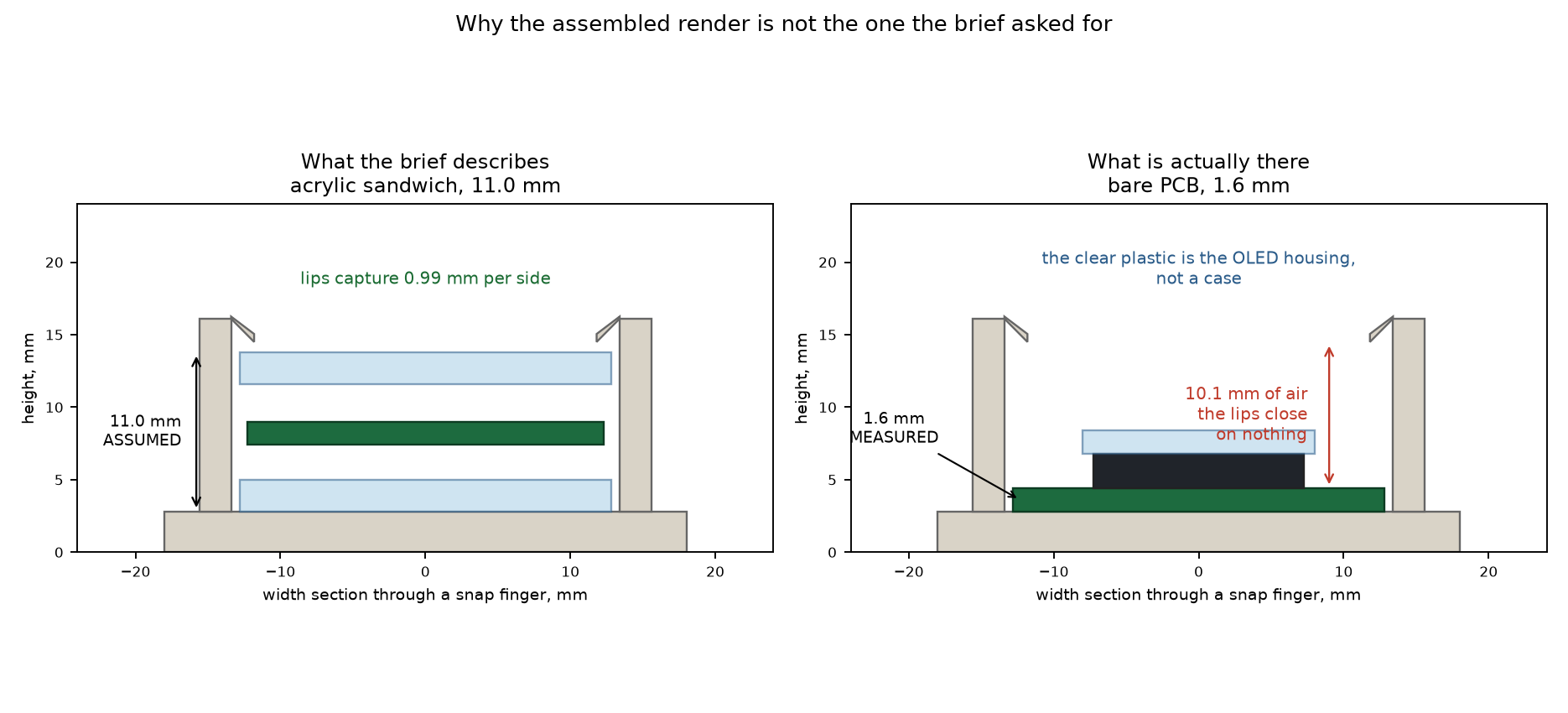
So the fingers on this page grip a stack that does not exist. The strain arithmetic below is correct and the print orientation is sound; they are simply the right answer to the wrong part. The next version grips the board edge instead, stays compliant across the range the photograph cannot resolve, and keeps zip ties as the actual retention — they are already holding this node up, which is a stronger argument than any snap calculation.
The dovetail rail, fixed rather than excused
The gate had been flagging the socket rails that the interchangeable feet slide onto, and it was right to. The rail was a 45-degree trapezoid that ran to a knife edge — 0.52 mm wide near the top, under the 0.84 mm practical minimum for this nozzle, thinning to nothing. It would have printed as a single stringy line or not at all.
It now stops where it still has a real face: a 0.90 mm flat top. That costs undercut height, so the matching tongue on each foot moved with it — widening to its shoulder lower down, where the capturing actually happens, then running straight up to carry the foot. Changing only the socket would have looked like a fix while quietly producing a dovetail that slides straight out.
Both feet now pass the gate with a full guarantee. Nothing here has been printed, so there were no printed parts to be made incompatible.
The gable head — a wide root instead of a slender arm
The earlier antenna arm looked brittle, and measuring it says it was. A slender arm is a cantilever with a small root, so the entire wind moment from the whip lands on one narrow section. The replacement is a full-width panel at the head of the board — a rectangular body with a triangle on top, tapering to a neck that carries the antenna at its peak.
The point is where the material is. The gable is widest at the bottom, where the bending moment is highest, and narrow only at the top, where it is lowest:
| old arm | gable | |
|---|---|---|
| root section | 9.0 × 2.8 mm | 33.0 × 13.0 mm |
| root stiffness, wind square-on | 16.5 mm⁴ | 6042 mm⁴ — ×367 |
| root stiffness, wind edge-on | — | 38932 mm⁴ — ×2365 |
Those are second moments of area of the root section — a geometric property, not a strength or fatigue prediction, and deliberately not presented as one.
It is also support-free by construction rather than by luck. The profile is drawn as a flat outline and extruded sideways, so every sloping face of the gable roof points upward — and an upward face is not an overhang at any angle. Printing it needs no supports anywhere, which was a hard requirement.
The antenna connector sits vertical at the peak: 8 mm of neck for its threads to bear on, opening into a 10 mm relief that runs down and out through the base so the nut can be reached from underneath.
rev2 — measured numbers, and a bay you can actually load
Two things arrived at once: real caliper numbers, and the discovery that the previous cradle could not be loaded. Both are in this revision.
The numbers first. The board is 2.0 mm thick, and from the bottom of the components hanging under it to the top of the board is 6.0 mm — so there is 4.0 mm of component depth underneath that has to float clear of anything. Standoffs are 5.0 mm, which clears them by a millimetre.
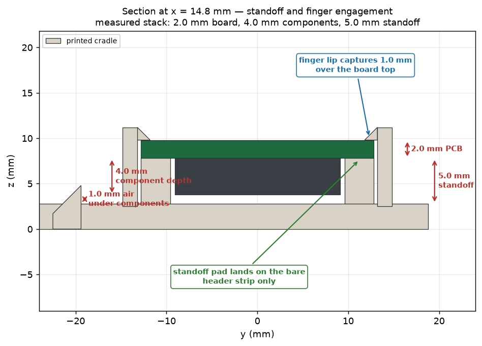
The second thing is blunter. The previous cradle's capture posts stood 16 mm tall with lips hooking inward at 14.5 mm. A 2 mm board cannot get past that from any direction — it could not be loaded at all. Those posts are gone. Measured on the exported mesh, the only material anywhere above the board is the four finger lips:
height above board top      material over the board
    0.3 mm                      13.52 mm2   <- the four lips
    0.8 mm                       0.00 mm2
    1.6 mm                       0.00 mm2
    3.0 mm                       0.00 mm2
    6.0 mm                       0.00 mm2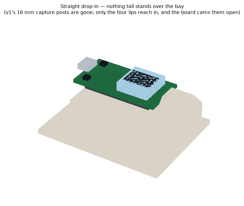
The fingers are solved rather than chosen: 1.633 mm thick over a 14 mm arm, which puts 1.50 % strain into the root against a 2.00 % limit for this plastic. They flex sideways in the print plane, so the bending runs along continuous extruded lines instead of trying to peel printed layers apart.
Both of the fit defects below are fixed in rev2, and both fixes are measured on the exported mesh rather than assumed. The antenna bore went from 50.1 % blocked to 0.0 %, clear through. The cable channel went from 16.8 of 23.3 mm too narrow to none of it, with 3.00 mm clear at the tightest point. The arm itself is otherwise unchanged — the shape was never the problem.
Still not printed. One item is flagged for a decision: the dovetail rails that the interchangeable feet slide onto taper to about 0.7 mm at their tips, a little under the practical minimum for this nozzle. It is inherited from the earlier version and it is marginal rather than broken, so it ships flagged rather than quietly changed.
Two more defects, found by putting the hardware in
Drawing the hardware into the model is a fit check, and this design had never had one. Everything above concerns the case that is not there. These two do not: they would still be defects if the acrylic sandwich were real.
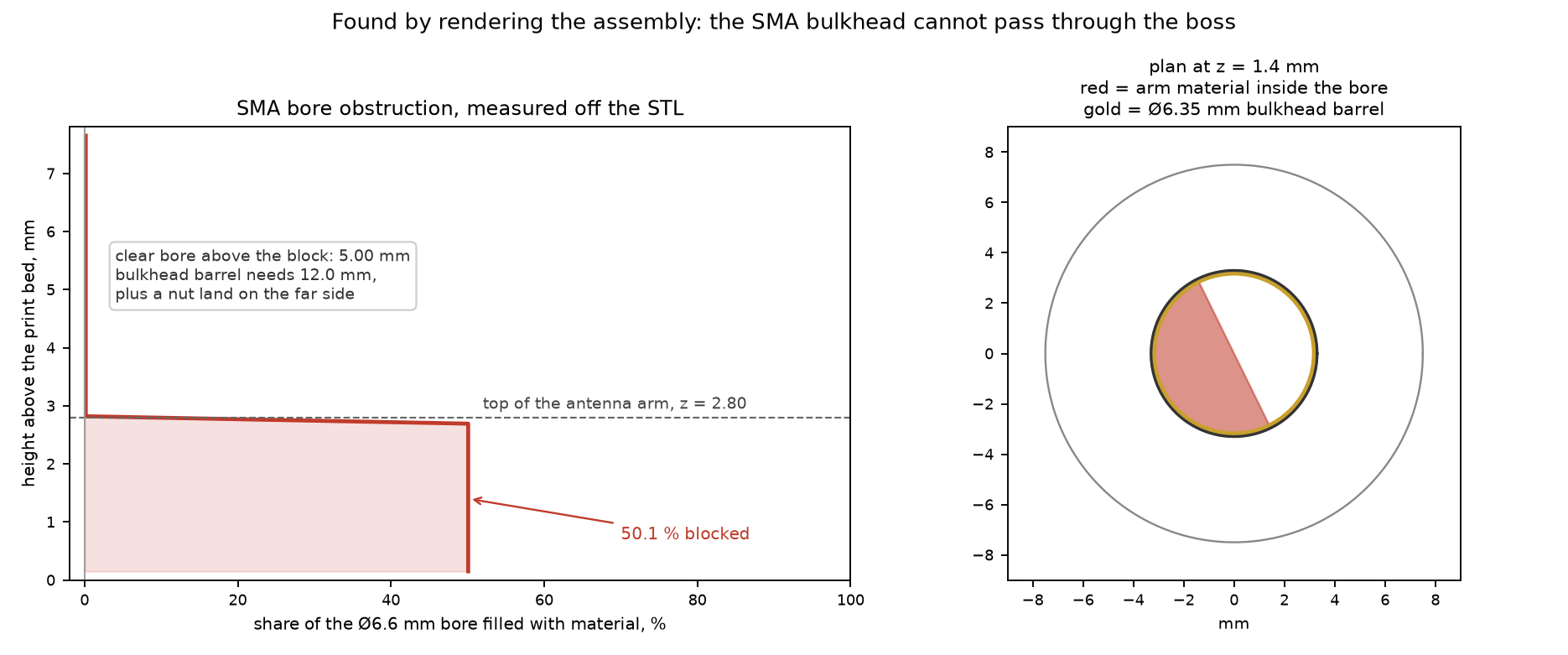
The antenna connector cannot be fitted. The bulkhead is supposed to drop through the boss and be held by a nut underneath. The arm that carries the boss terminates on the bore's centreline, which leaves the hole 50.1% filled with solid plastic below 2.80 mm and only 5.00 mm of clear bore above it. The barrel is about 12 mm long and the nut needs a face to land on. Neither exists, and no amount of pushing changes that.
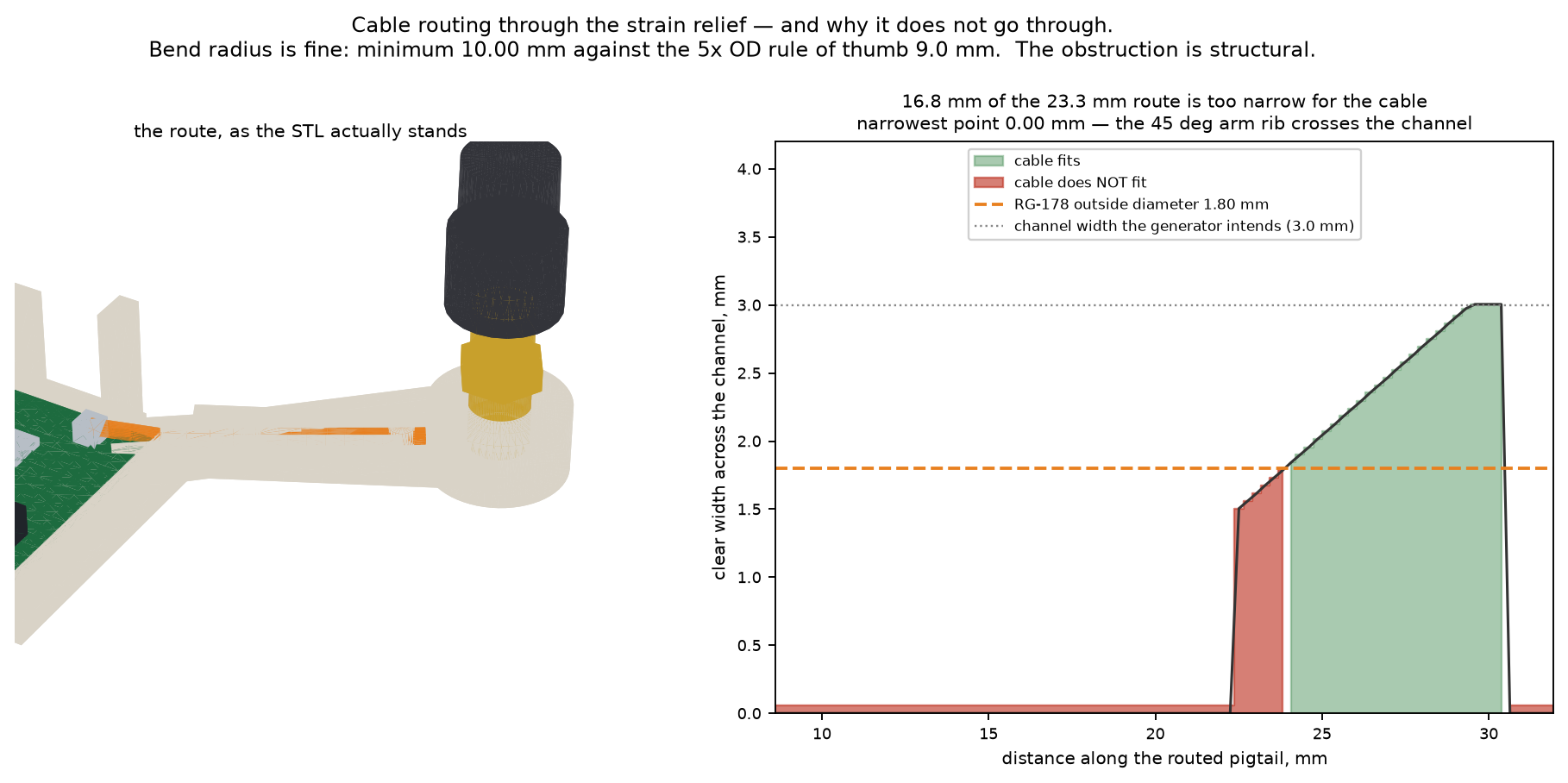
The coax cannot go through its own channel. The strain-relief walls are placed 3.0 mm apart, which is right for the cable. What nothing checked is whether the space between the walls stays clear along its length. It does not: a stiffening rib on the antenna arm sits about sixteen degrees off the arm's axis — nearly parallel to the cable route — so it does not cross the channel, it runs down the middle of it. 16.8 mm of the 23.3 mm route is narrower than the cable, and at its worst the route is completely solid.
The irony is that the bend radius, which is the thing the brief was anxious about and the reason the channel exists at all, is fine: the route holds a 10.0 mm minimum radius against a rule-of-thumb minimum of 9.0 mm. The fragile connector was protected. The cable just cannot get there.
The dimension that started it
| dimension | value | basis |
|---|---|---|
| Case width | 25.6 mm | measured caliper, cross-checked against the published board width |
| Board length | 50.7 mm | published bare board — and the board is bare, so there is no overhang to add |
| Board thickness | 1.6 mm | measured 0.5–1.5 mm off the photo against a 2.54 mm header pitch; 1.6 mm is the standard value it brackets |
| Case stack thickness | n/a | withdrawn there is no case — see the correction above |
Print settings
- PETG, 0.4 mm nozzle, 0.20 mm layers, A1 Mini.
- 4 walls for snap durability and SMA boss strength; 5 top/bottom layers.
- 30–40% gyroid infill; 50% for the ground spike in hard soil.
- Supports off. Overhanging lips and interfaces are modelled as ~45° ramps, and the pole foot uses a V-block rather than a round bore specifically to avoid support-heavy geometry.
Related
The companion app for this hardware reads signal data, GPS and coverage over Bluetooth; its privacy policy — the app collects nothing — is at LoRa Tracker privacy policy.
Other prints: 3D Printed Projects, and RONDO, a slide rule on a print-in-place bearing.